


Breaking News
 The Hybrid Semi-Truck Is Real: Big Updates from Environment Canada
 Public schools are imploding by 1.5 million kids as parents seek alternatives...
 Securing Peace with Iran Compels Trump to Divorce Israel
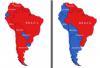 Seven 'far-right' candidates have won in Latin America since USAID was defunded…
Top Tech News
 World's first consumer wing-in-ground effect aircraft takes flight
 America's Military Readiness Depends On Deployable Nuclear Power
 License Plate Cameras Are About To Start Tracking A Lot More Than Just Your Car
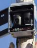 Heads up: Apparently the government is hiding cameras inside fake utility boxes
 Sodium Batteries And EVs That Power The Grid: Inside GM's Big Energy Push
 NUCLEAR ENGINE - UNLIMITED LUXURY - 20 YEARS WITHOUT REFUELING
 China Unveils Nuclear-Powered Floating Hub For Green Shipping
 China Launches World's 1st Commercial Brain Chip, Beating Elon Musk's Neuralink!
 Modular next-gen US nuclear reactor goes critical
 How EMF's cause disease


Taiwan Semiconductor will have volume production of 7 nanometer chips...
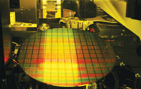
The foundry also described enhancements to its two chip-stacking techniques, advances in RF CMOS and work in transistors and materials, paving the way to a 3nm node and beyond. In addition, it previewed design capabilities using machine learning that it will offer before the end of the year.
Among its achievements, TSMC noted 76 percent yields on the 256Mbit SRAM made in its first-generation 7nm node, which will be in volume production next year. It also reported that an ARM Cortex-A72 processor in the node exceeded 4GHz using a new design flow.
The Taiwan company, already the world's largest foundry by far, expects to ship 11 million 12-inch-equivalent wafers this year, a typical 10 percent annual increase. The biggest share—two million wafers—will use its planar 28nm processes for which it is boosting capacity 15 percent this year.