


Breaking News
 Is 'Project Freedom' Just Another Trump Scam?
 THEY LIED About the Water - THE WELLS ARE GOING DRY GLOBALLY
 After Attack of Cargo Vessel, Trump Directs US to Escort Foreign Ships Through Hormuz
 RED ALERT: "I Think That You're Gonna See Billions Dead At This Rate!"
Top Tech News
 Robot Dives 1.5 Miles, Maps French Shipwreck With 86,000 Images And Recovers Artifacts
 Brain-inspired chip could reduce AI energy use by 70%
 CANCER HAS BEEN CURED
 "This is the first synthetic species," microbiologist J. Craig Venter told 60 Minutes'
 Humanoid robots are hitting the factories at an increasing pace
 Microsoft's $400 Billion Mistake Is Now a $200 Phone With Zero Tracking
 Turn Sand to Stone With Vinegar. Stronger Than Steel. Hidden Since 1627
 This is a bioprinter printing with living human cells in real time
 The remarkable initiative is called The Uncensored Library,...
 Researcher wins 1 bitcoin bounty for 'largest quantum attack' on underlying tech


Taiwan Semiconductor Will Have Volume Production of 3 Nanometer Chips in 2022
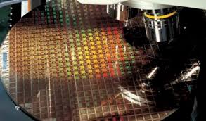
TSMC was the first company to use ASML's EUV lithography machines for high-volume production and now has at least three processes that use EUV for select layers. They use EUV lithography for its N7+, N6, and N5 nodes.
TSMC's 2nd generation 7 nm technology (N7+) uses EUV for up to four layers in order to reduce its use of multi-patterning techniques when building highly complex circuits. The 6 nm process (N6) is for customers to re-use IP designed for 1st generation 7 nm, per the report. TSMC's 5 nm process (N5) can use EUV for up to 14 layers. 5nm has significant increase in transistor density and performance enhancements.
2nd generation 5 nm (N5P) and 4 nm (N4) fabrication processes are based 5 nm technology and will have performance and power benefits. N5P will be available in 2021. N4 chips will have volume production in 2022.
Next-generation 3 nm process (N3) will be a full node improvement over N5. N3 will have 70 percent logic density gain, 15-percent performance gain, and 30-percent power reduction over the 5-nm process. N3 will use EUV over 20 layers.
Nextbigfuture covered Taiwan Semiconductors plans from 2017. TSMC has kept on track with its Moore's Law roadmap to reach 3-nanometer chips by 2022.