


Breaking News
 DON MESS WITH ME Trump says Iran will 'be blown off face of earth' if they attack US warship
 Digital ID: Treasury Secretary Scott Bessent Reveals Trump Plans To Sign Executive Order To Hand...
 Pardon or not, there's one very dire reason why Fauci must be charged quickly…
 The Spanish-US Spat Could Lead To NATO's Unraveling
Top Tech News
 Robot Dives 1.5 Miles, Maps French Shipwreck With 86,000 Images And Recovers Artifacts
 Brain-inspired chip could reduce AI energy use by 70%
 CANCER HAS BEEN CURED
 "This is the first synthetic species," microbiologist J. Craig Venter told 60 Minutes'
 Humanoid robots are hitting the factories at an increasing pace
 Microsoft's $400 Billion Mistake Is Now a $200 Phone With Zero Tracking
 Turn Sand to Stone With Vinegar. Stronger Than Steel. Hidden Since 1627
 This is a bioprinter printing with living human cells in real time
 The remarkable initiative is called The Uncensored Library,...
 Researcher wins 1 bitcoin bounty for 'largest quantum attack' on underlying tech


Taiwan Semiconductors Future Lithography
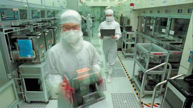
The more advanced 2nm process is also reported to have made significant progress. The 2nm process will start mass production around 2023 to 2024.
TSMC thinks risk trial production yield in the second half of 2023 can reach 90%. The 3nm and 5nm processes use FinFET. TSMC 2nm process uses a new multi-bridge channel field effect transistor (MBCFET) architecture.
TSMC plans to switch to GAAFET (gate all around) for 2nm chips. FINFET doesn't surround a channel on all sides. GAA surrounds a channel using a Gate. The latter method makes current leakage almost negligible.
The N5 node that TSMC is working with can use 5nm for up to 14 layers. The 3nm process node could deliver up to a 15% hike in power at the same transistor count as 5nm, and up to a 30% reduction in power use (at the same clock speeds and complexity).
Dutch lithography company ASML says that at 3nm, lithography can be used on more than 20 layers.
Intel is lagging TSMC in reducing transistor size. Intel has published a roadmap that reaches 1.4 nanometers in 2029.