


Breaking News
 Does AIPAC really have too much power?
 California Is Facing A "Fuelmaggedon" As Fighting Erupts In The Middle East And The Strait
 Grand Theft World Podcast 285 | Ba'alroom Psyops with Guest Ryan Graham
 Why Socialism Fails
Top Tech News
 Robot Dives 1.5 Miles, Maps French Shipwreck With 86,000 Images And Recovers Artifacts
 Brain-inspired chip could reduce AI energy use by 70%
 CANCER HAS BEEN CURED
 "This is the first synthetic species," microbiologist J. Craig Venter told 60 Minutes'
 Humanoid robots are hitting the factories at an increasing pace
 Microsoft's $400 Billion Mistake Is Now a $200 Phone With Zero Tracking
 Turn Sand to Stone With Vinegar. Stronger Than Steel. Hidden Since 1627
 This is a bioprinter printing with living human cells in real time
 The remarkable initiative is called The Uncensored Library,...
 Researcher wins 1 bitcoin bounty for 'largest quantum attack' on underlying tech


Ion beam controlled to etch single silicon atom depth
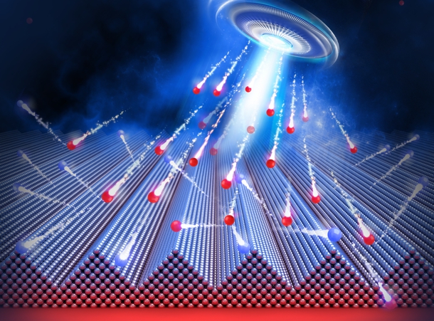
The beams can create tiny features in the lateral dimensions—length and width, but to create the next generation of nanometer-scale devices, the energetic ions must precisely control the features in the vertical dimension—depth. Now, researchers at the National Institute of Standards and Technology (NIST) have demonstrated that a standard ion-beam technique can be fine-tuned to make structures with depths controlled to within the diameter of a single silicon atom.
Above – nanofluidic staircase machined with subnanometer precision by a focused ion beam separates nanoparticles by size. The device is also a reference material to accurately measure nanoparticle size and compare it to optical brightness, which could aid in the quality control of consumer products. Credit: NIST