


Breaking News
 Netanyahu has a plan to undermine President Trump, and it includes Fox News…
 The Brits Should Declare Their Independence, Too
 The Last Places in America That Might Survive the Collapse
 Swap Lines, Secret Bailouts, and the Weaponization of the Dollar
Top Tech News
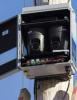 Heads up: Apparently the government is hiding cameras inside fake utility boxes
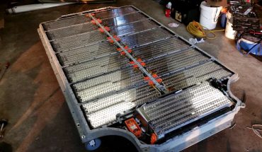
 Sodium Batteries And EVs That Power The Grid: Inside GM's Big Energy Push
 NUCLEAR ENGINE - UNLIMITED LUXURY - 20 YEARS WITHOUT REFUELING
 China Unveils Nuclear-Powered Floating Hub For Green Shipping
 China Launches World's 1st Commercial Brain Chip, Beating Elon Musk's Neuralink!
 Modular next-gen US nuclear reactor goes critical
 How EMF's cause disease
 This Company Will Add Phone, AirPod, and Smartwatch Trackers to License Plate Readers
 Elon Details SpaceX AI Data Center in Space Details and Roadmap
 5-in-1 miniature surgical robot is the size of a seed


Finally, Commercialization of Wafers of Carbon Nanotube Transistor Chips
CNFETs are more energy-efficient than silicon field-effect transistors and could be used to build new types of three-dimensional microprocessors.
They found that dry cycling, a method of intermittently drying out the submerged wafer, could dramatically reduce the incubation time — from 48 hours to 150 seconds.
After analyzing the deposition technique used to make the CNFETs, Max Shulaker, an MIT assistant professor of electrical engineering and computer science, and his colleagues made some changes to speed up the fabrication process by more than 1,100 times compared to the conventional method, while also reducing the cost of production. The technique deposited carbon nanotubes edge to edge on the wafers, with 14,400 by 14,400 arrays CFNETs distributed across multiple wafers.
A 3D computer chip with combined logic and memory functions is projected to "beat the performance of a state-of-the-art 2D chip made from silicon by orders of magnitude.
Abstract
Carbon nanotube field-effect transistors (CNFETs) are a promising nanotechnology for the development of energy-efficient computing. Despite rapid progress, CNFETs have only been fabricated in academic or research laboratories. A critical challenge in transferring this technology to commercial manufacturing facilities is developing a suitable method for depositing nanotubes uniformly over industry-standard large-area substrates. Such a deposition method needs to be manufacturable, compatible with today's silicon-based technologies, and provide a path to achieving systems with energy efficiency benefits over silicon. Here, we show that a deposition technique in which the substrate is submerged within a nanotube solution can address these challenges and can allow CNFETs to be fabricated within industrial facilities.