


Breaking News
 The Judaism-Zionism Bifurcation: Tikkun Olam: Fixing The World, But For What, For Whom?
 The Trump Hustle
 Aww... Look At The Cute Dancing-Robot Police-State Surveillance-Dog...
 "Working Better": Saylor Teases BTC Buy After Strategy Sells For First Time Since 2022
Top Tech News
 Elon and SpaceX Have Made AI Training 10 Times Faster
 Oklo COO Says Nuclear Waste Could Power America For 150 Years
 SpaceX Announces LARGEST Starship Mission Ever! They've never done this before!
 Cars Are Fast Becoming Dystopian Prison Pods...
 Our Emergency Water Plan Wasn't Good Enough - So We Built This
 Sodium Ion Batteries Can Reach 100 Gigawatt Per Hour Per Year Scale in 2027
 Juiced Bikes proves capable electric motorcycles don't have to cost a lot
 Headlight projectors turn your car into a drive-in theater
 US To Develop Small Modular Nuclear Reactors For Commercial Shipping
 New York Mandates Kill Switch and Surveillance Software in Your 3D Printer ...


Laser-driven Particle Accelerator Made Ten Thousand Times Smaller
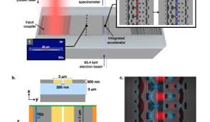
Current implementations of DLAs rely on free-space lasers directly incident on the accelerating structures, limiting the scalability and integrability of this technology. Researchers present the first experimental demonstration of a waveguide-integrated DLA, designed using a photonic inverse design approach. These on-chip devices accelerate sub-relativistic electrons of initial energy 83.4 keV by 1.21 keV over 30 µm, providing peak acceleration gradients of 40.3 MeV/m. This progress represents a significant step towards a completely integrated MeV-scale dielectric laser accelerator.
Dielectric laser accelerators have emerged as a promising alternative to conventional RF accelerators due to the large damage threshold of dielectric materials the commercial availability of powerful NIR femtosecond pulsed lasers, and the low-cost high-yield nanofabrication processes which produce them. Together, these advantages allow DLAs to make an impact in the development of applications such as tabletop free-electron-lasers, targeted cancer therapies, and compact imaging sources.