


Breaking News
 Is 'Project Freedom' Just Another Trump Scam?
 THEY LIED About the Water - THE WELLS ARE GOING DRY GLOBALLY
 After Attack of Cargo Vessel, Trump Directs US to Escort Foreign Ships Through Hormuz
 RED ALERT: "I Think That You're Gonna See Billions Dead At This Rate!"
Top Tech News
 Robot Dives 1.5 Miles, Maps French Shipwreck With 86,000 Images And Recovers Artifacts
 Brain-inspired chip could reduce AI energy use by 70%
 CANCER HAS BEEN CURED
 "This is the first synthetic species," microbiologist J. Craig Venter told 60 Minutes'
 Humanoid robots are hitting the factories at an increasing pace
 Microsoft's $400 Billion Mistake Is Now a $200 Phone With Zero Tracking
 Turn Sand to Stone With Vinegar. Stronger Than Steel. Hidden Since 1627
 This is a bioprinter printing with living human cells in real time
 The remarkable initiative is called The Uncensored Library,...
 Researcher wins 1 bitcoin bounty for 'largest quantum attack' on underlying tech


TSMC will starting full EUV lithography of 5 nanometer chips April 2019
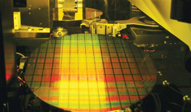
The foundry's update showed that area and power gains continue in its leading-edge nodes, but chip speeds are no longer advancing at their historic rate. To compensate, TSMC gave an update on a half-dozen packaging techniques that it is developing to speed connections between chips.
The TSMC N7+ node that can use EUV on up to four layers. Its N5 that will use EUV on up to 14 layers will be ready for risk production in April. EUV aims to lower costs by reducing the number of masks required for leading-edge designs.
Samsung is ramping a 7-nm node using EUV. Intel is not expected to use EUV anytime soon. Globalfoundries announced in August that it has halted work on 7 nm and EUV.