


Breaking News
 The current "UFO/UAP disclosure" campaign is not a grassroots or independent effort.
 Scientists Discover A 113-million-year-old Pterosaur Wing Preserved In Extraordinary Detail
 States Finally Begin to Roll Back Free Healthcare for Illegal Aliens
 Trump's ready to reopen mental institutions and liberals are furious…
Top Tech News
 Heads up: Apparently the government is hiding cameras inside fake utility boxes
 Sodium Batteries And EVs That Power The Grid: Inside GM's Big Energy Push
 NUCLEAR ENGINE - UNLIMITED LUXURY - 20 YEARS WITHOUT REFUELING
 China Unveils Nuclear-Powered Floating Hub For Green Shipping
 China Launches World's 1st Commercial Brain Chip, Beating Elon Musk's Neuralink!
 Modular next-gen US nuclear reactor goes critical
 How EMF's cause disease
 This Company Will Add Phone, AirPod, and Smartwatch Trackers to License Plate Readers
 Elon Details SpaceX AI Data Center in Space Details and Roadmap
 5-in-1 miniature surgical robot is the size of a seed


Breakthrough could triple the energy collected by solar to 60% efficiency
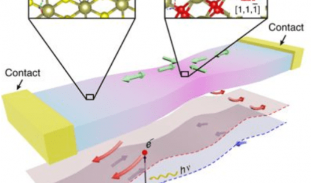
UK researchers can now 'funnel' electrical charge onto a chip. Using the atomically thin semiconductor hafnium disulphide (HfS2), which is oxidized with a high-intensity UV laser, the team were able to engineer an electric field that funnels electrical charges to a specific area of the chip, where they can be more easily extracted.
This method has the potential to harvest three times the energy compared with traditional systems. The researchers believe their breakthrough could result in solar panels, no bigger than a book, producing enough energy to power a family-sized house.

Abstract – Strain-engineered inverse charge-funnelling in layered semiconductors
The control of charges in a circuit due to an external electric field is ubiquitous to the exchange, storage and manipulation of information in a wide range of applications. Conversely, the ability to grow clean interfaces between materials has been a stepping stone for engineering built-in electric fields largely exploited in modern photovoltaics and opto-electronics.