


Breaking News
 The current "UFO/UAP disclosure" campaign is not a grassroots or independent effort.
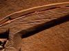 Scientists Discover A 113-million-year-old Pterosaur Wing Preserved In Extraordinary Detail
 States Finally Begin to Roll Back Free Healthcare for Illegal Aliens
 Trump's ready to reopen mental institutions and liberals are furious…
Top Tech News
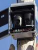 Heads up: Apparently the government is hiding cameras inside fake utility boxes
 Sodium Batteries And EVs That Power The Grid: Inside GM's Big Energy Push
 NUCLEAR ENGINE - UNLIMITED LUXURY - 20 YEARS WITHOUT REFUELING
 China Unveils Nuclear-Powered Floating Hub For Green Shipping
 China Launches World's 1st Commercial Brain Chip, Beating Elon Musk's Neuralink!
 Modular next-gen US nuclear reactor goes critical
 How EMF's cause disease
 This Company Will Add Phone, AirPod, and Smartwatch Trackers to License Plate Readers
 Elon Details SpaceX AI Data Center in Space Details and Roadmap
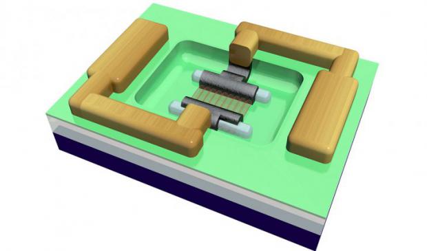
 5-in-1 miniature surgical robot is the size of a seed


IBM has made Carbon nanotubes transistors smaller and faster than silicon
Now IBM and others will have to scale up superior carbon nanotube devices.
IBM scientists have been experimenting with carbon nanotubes, rolled-up sheets of carbon atoms just 1 nanometer, or a billionth of a meter, in diameter. But difficulties working with the material have meant that, for optimal performance, nanotube transistors have to be even larger than current silicon transistors, which are about 100 nanometers across. To cut that number down, a team of scientists used a new technique to build the contacts that draw current into and out of the carbon nanotube transistor. They constructed the contacts out of molybdenum, which can bond directly to the ends of the nanotubes, making them smaller. They also added cobalt so the bonding could take place at a lower temperature, allowing them to shrink the gap between the contacts. Another advance allowed for practical transistors.