


Breaking News
 The current "UFO/UAP disclosure" campaign is not a grassroots or independent effort.
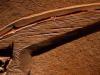 Scientists Discover A 113-million-year-old Pterosaur Wing Preserved In Extraordinary Detail
 States Finally Begin to Roll Back Free Healthcare for Illegal Aliens
 Trump's ready to reopen mental institutions and liberals are furious…
Top Tech News
 Heads up: Apparently the government is hiding cameras inside fake utility boxes
 Sodium Batteries And EVs That Power The Grid: Inside GM's Big Energy Push
 NUCLEAR ENGINE - UNLIMITED LUXURY - 20 YEARS WITHOUT REFUELING
 China Unveils Nuclear-Powered Floating Hub For Green Shipping
 China Launches World's 1st Commercial Brain Chip, Beating Elon Musk's Neuralink!
 Modular next-gen US nuclear reactor goes critical
 How EMF's cause disease
 This Company Will Add Phone, AirPod, and Smartwatch Trackers to License Plate Readers
 Elon Details SpaceX AI Data Center in Space Details and Roadmap
 5-in-1 miniature surgical robot is the size of a seed


Towards roll to roll graphene production

A team of engineers from Exeter's Centre for Graphene Science have developed a new method for creating entire device arrays directly on the copper substrates used for the commercial manufacture of graphene. Complete and fully-functional devices can then be transferred to a substrate of choice, such as silicon, plastics or even textiles.
Professor David Wright, from Exeter's Engineering department and one of the authors said: "The conventional way of producing devices using graphene can be time-consuming, intricate and expensive and involves many process steps including graphene growth, film transfer, lithographic patterning and metal contact deposition. Our new approach is much simpler and has the very real potential to open up the use of cheap-to-produce graphene devices for a host of important applications from gas and bio-medical sensors to touch-screen displays."